2017 High-Resolution Spin-on-Patterning of Perovskite Thin Films for a Multiplexed Image Sensor Array
본문
- Journal
- Advanced Materials
- Vol
- 29
- Page
- 1702902
- Year
- 2017
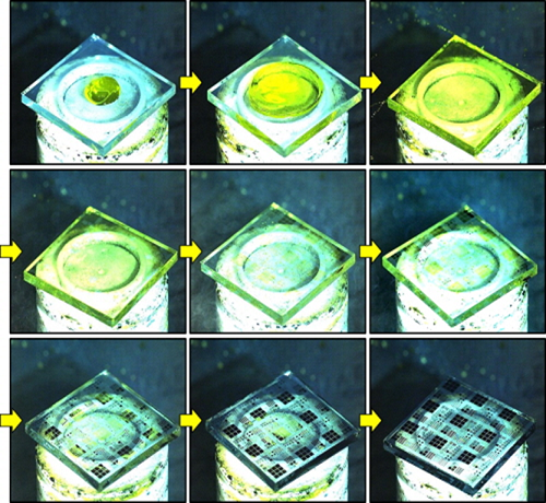
Inorganic–organic hybrid perovskite thin films have attracted significant attention as an alternative to silicon in photon-absorbing devices mainly because of their superb optoelectronic properties. However, high-definition patterning of perovskite thin films, which is important for fabrication of the image sensor array, is hardly accomplished owing to their extreme instability in general photolithographic solvents. Here, a novel patterning process for perovskite thin films is described: the high-resolution spin-on-patterning (SoP) process. This fast and facile process is compatible with a variety of spin-coated perovskite materials and perovskite deposition techniques. The SoP process is successfully applied to develop a high-performance, ultrathin, and deformable perovskite-on-silicon multiplexed image sensor array, paving the road toward next-generation image sensor arrays.

